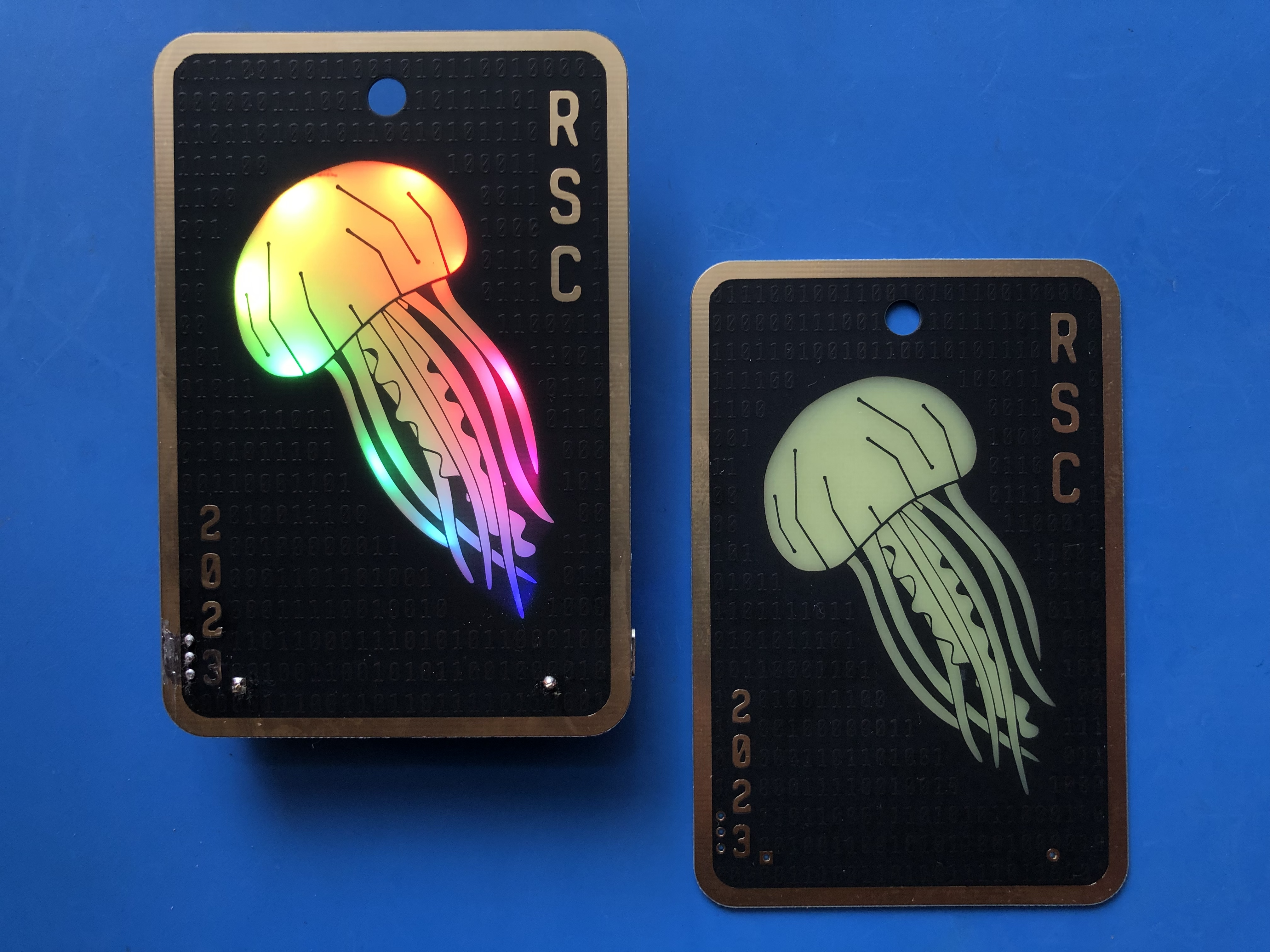
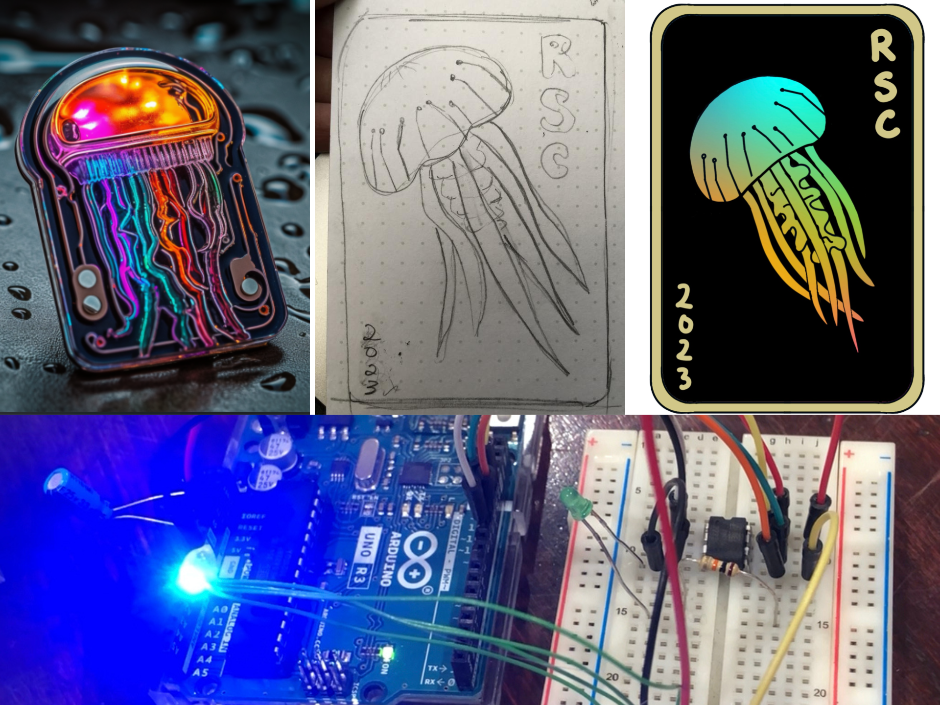
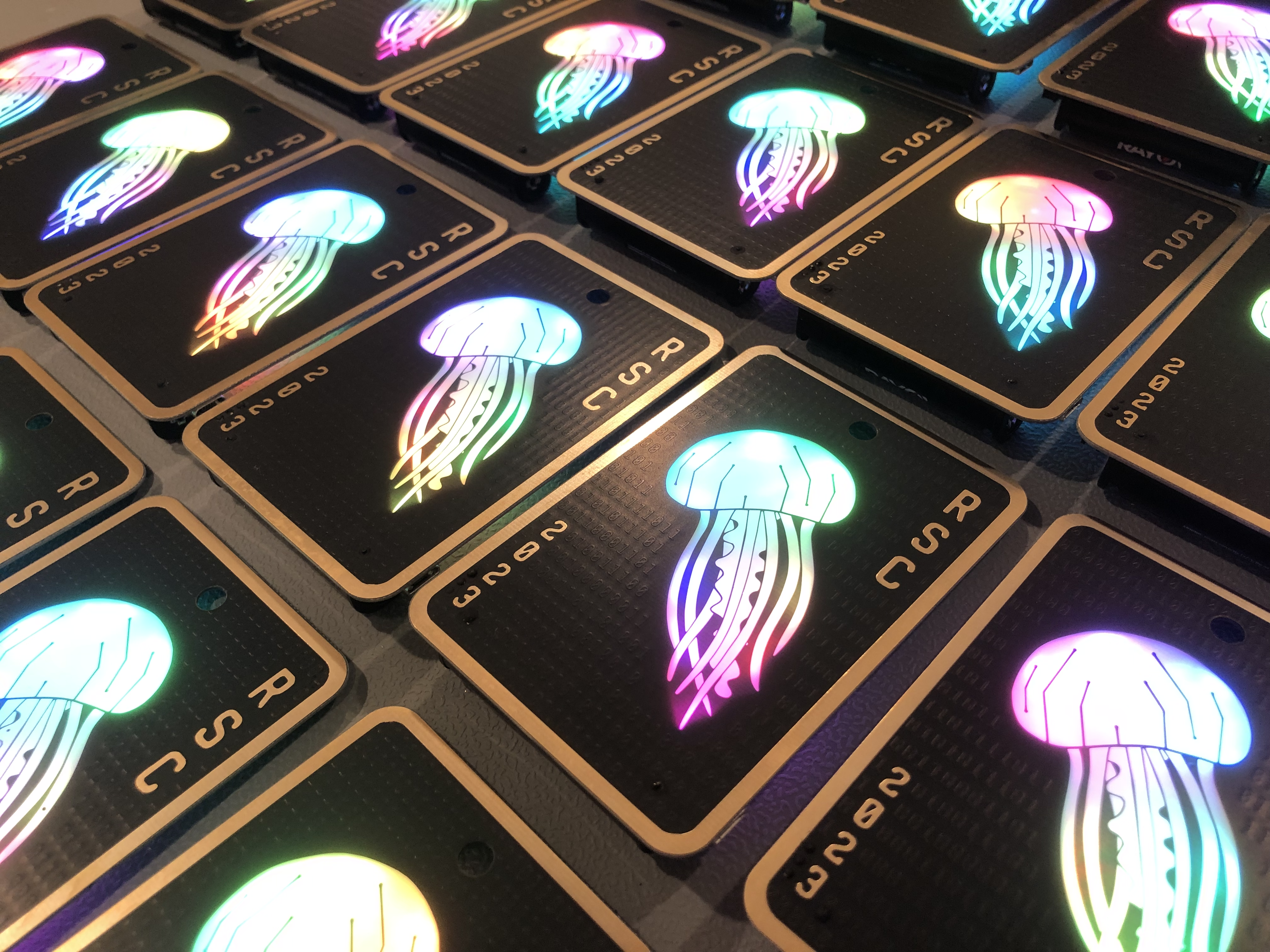
This blog post series will cover the journey from start to finish in making a “badge” (PCB art) for the Red Society Discord. Or, it will at least cover the useful parts. : )
Red Society Club is a welcoming infosec community hosted on Discord, our invite link is here: https://discord.gg/theRSC
Printed circuit board art?!
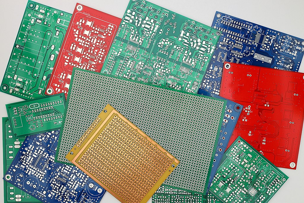
PCBs (printed circuit boards) are the heart of modern electronics. They’re in your phones, cars, dishwashers… though they aren’t necessarily known for their beauty.
But, somewhere along the way, someone took the practice of PCB design–a typically staid and utilitarian skill–and used it to make something artistic. And thus, PCB art was born.
This is most commonly seen in DEFCON’s “badgelife” scene, but you’ll find it at other infosec and hardware conferences as well. And, its popularity has spilled over into kits for hobbyists and kids, such as those found at Adafruit and Tindie.
Okay, but why?
My initial answer is “why not?”
Most of these projects are just for fun. You’ll see some that are purely artistic endeavors, ranging from the very simple to the very complex. Some have built-in games or other functionality.
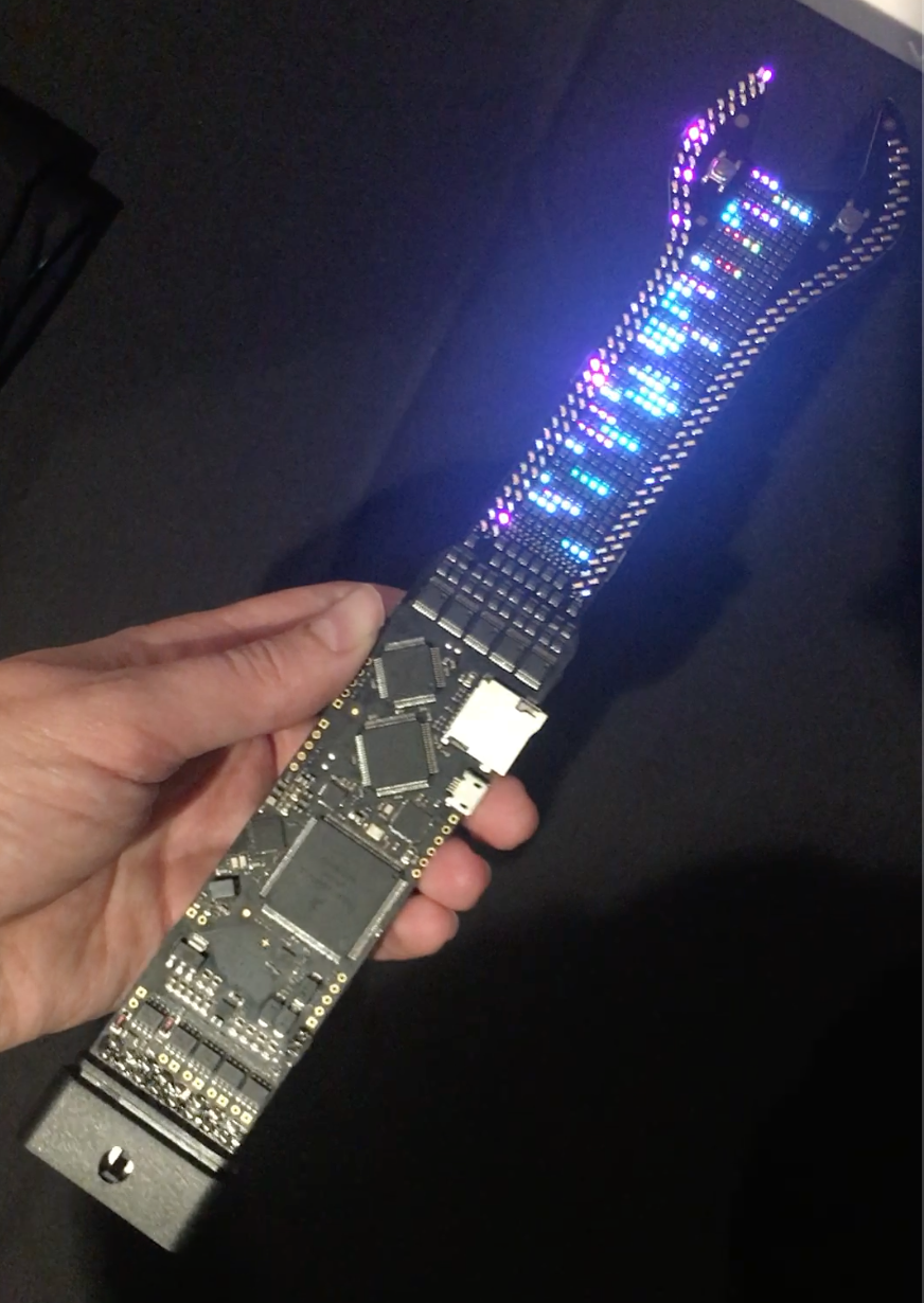
And a few of them, like DEFCON 26’s CHV badge, double as a fully functional tool (in this case, an OBD-II port).
In the case of this specific board, we wanted to make an artistic badge that would look cool sitting on a desk, and also celebrate the start of our Discord group.
PCB art styles
With art being our main priority for this project, let’s look at some art styles:
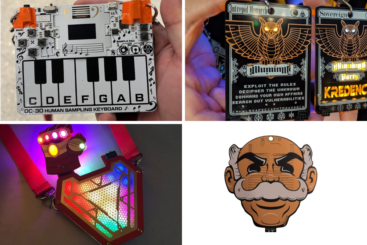
Upper left: Defcon 30 badge, upper right: Illuminati badge by Kredence, lower left: Arc badge by TwinkleTwinkie, lower right: Mr. Robot badge by Benchoff.
You can see there are a lot of different art styles in “badgelife” badges.
There are some color limitations, including soldermask, which is the (typically) green epoxy or polymer coating. But you can get other colors too, including red, purple, blue, black, and even clear over black.
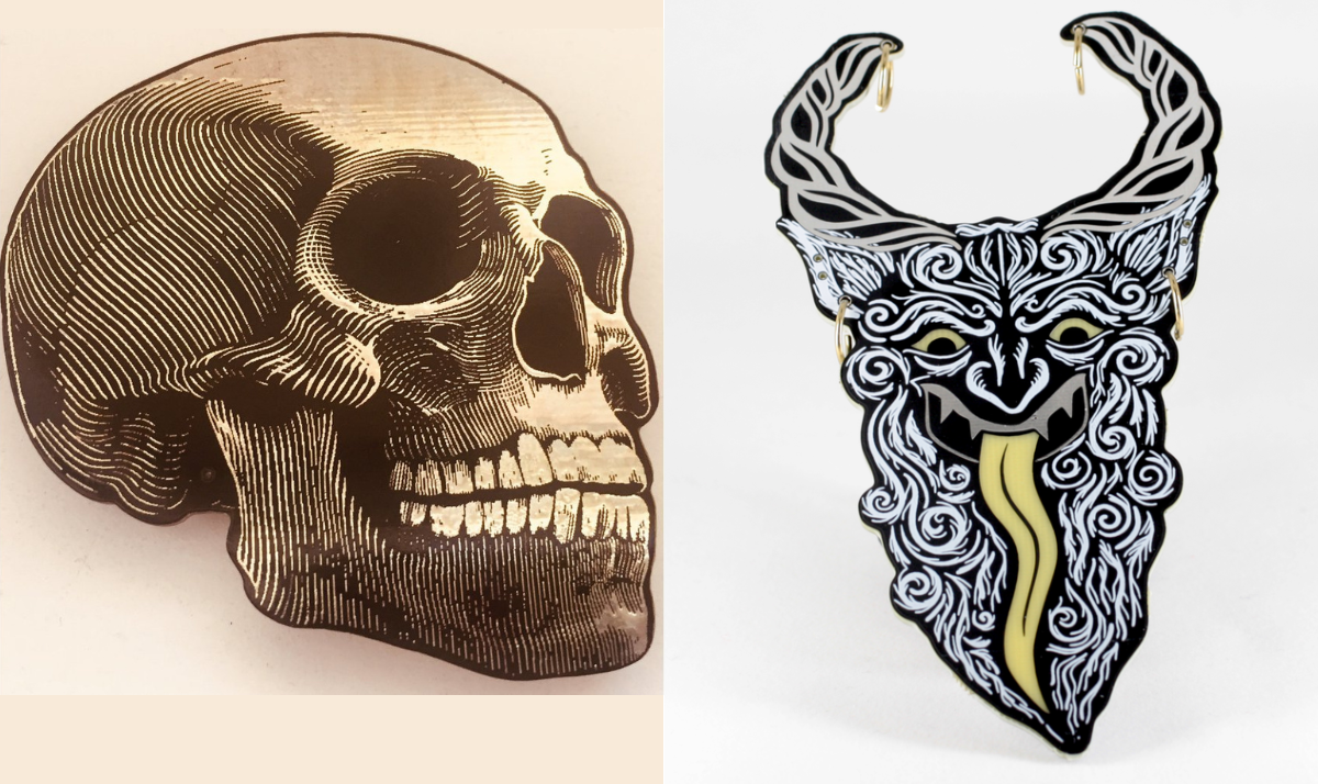
From there, you can add silkscreen, typically in white. You can make some really beautiful artwork with soldermask and silkscreen, such as this half-tone piece by nerfhammer (left) or Krampus by Alpenglow Industries (right).
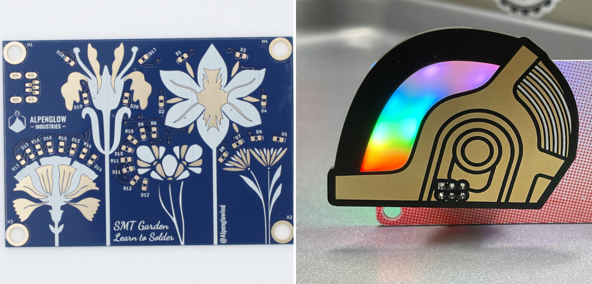
From an artistic standpoint, you can get another color by exposing the copper layer. This can have a copper, gold, or silver color to it depending on the finish. SMT Garden by Alpenglow Industries on the left, and Daft Punk SAO by TwinkleTwinkie on the right.
Last but not least: coloring with light. You can have a ton of LEDs on the front and create color that way, or you can have exposed FR4 (the “filler” material in the middle of a PCB, that separates copper layers) with light shining through it. On the right is a badge by ANDnXOR and on the left are several badges by BadgePirates.
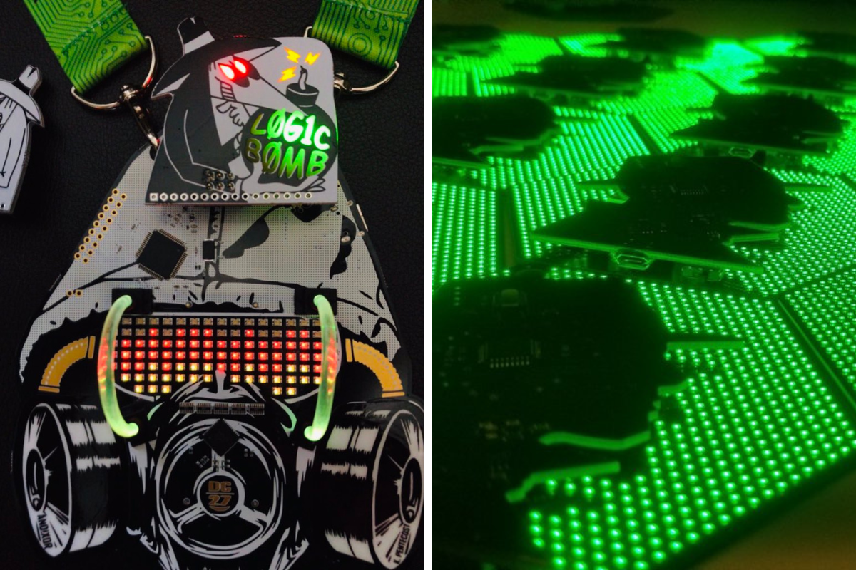
This backlit style is what we’ll focus on for the RSC badge, because I love how it looks:
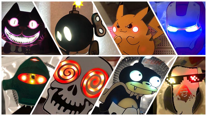
The artwork for these boards has to be separated into different layers representing the PCB’s layers. This can be done with a tool such as Svg2Shenzhen. We’ll see this process in more detail in later blog posts.
Our goals
For this board (and for this blog post series!) we have a few ideas in mind:
-
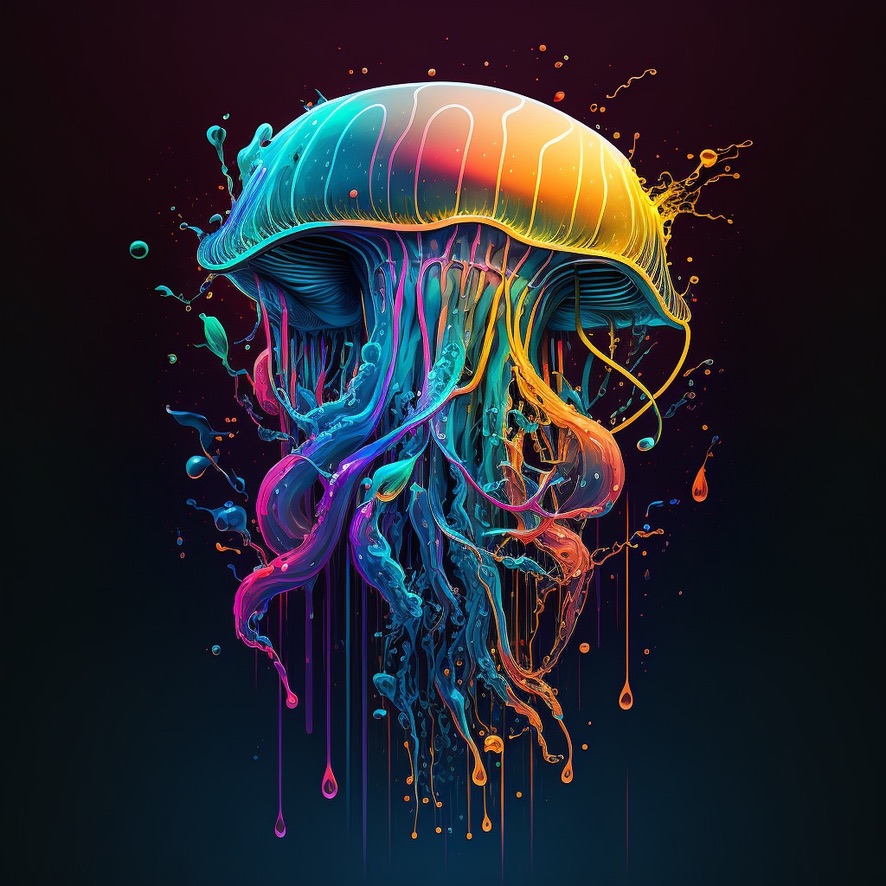
We want to make a PCB badge of a jellyfish. Why a jellyfish? It’s the icon of the admin who came up with the idea (shoutout to Ang!).
-
Last but not least, I want to keep things relatively simple so I can get it done in the few months before DEFCON, while also having a lot of life and work stuff going on.
That doesn’t leave us with a lot of constraints. While that sounds nice, I’m the type of person who is typically helped by constraints. I find it much easier to have a challenging set of constraints that forces some out of the box thinking, compared to a completely blank canvas.
In our case, our own constraints are: must include jellyfish, LEDs, nothing too crazy. That rules out more interesting stuff like Bluetooth, screens, games (capacitive touch) and other inter-badge communication that you see on the main DEFCON badges.
Plus, I’ve wanted to do a design with reverse-mount LEDs for quite a while.

But even those constraints leave things pretty wide open. What style of art will it have? What colors will be there? Can people easily change the software?
Other constraints you might have in a design include: keeping the BOM (bill of materials) under a certain cost, timelines, art styles.
The PCB design process
If you are making a board, the overall process looks like this:
- Ideation (what we’ve already talked about in this post)
- Prototyping/breadboarding
- KiCad schematic + board layout
- First “board spin”: order a set of PCBs, assemble and test
- Fix any issues
- Another board spin if needed*
- Fix any issues, repeat until you have a final product or you run out of time.
*And it will be needed
The later in the process you find issues, the more expensive they are to fix.
All other things equal, you want to figure out as many problems in the prototyping/breadboarding phase as possible, even if it’d be more fun to move onto the next steps.
The prototyping/breadboarding phase will be where you try to anticipate, test, and fix as many design issues as possible while things are still impermanent (at least, impermanent relative to circuit design).
Once you think you’ve found and fixed all the issues, the next step is to have some PCBs made. Here you’ll see how theory butts up against reality, and then find and fix any remaining issues.
And if all goes well, we’ll have boards in hand in time for DEFCON!
In the next post, we’ll cover the initial prototyping of our board.
