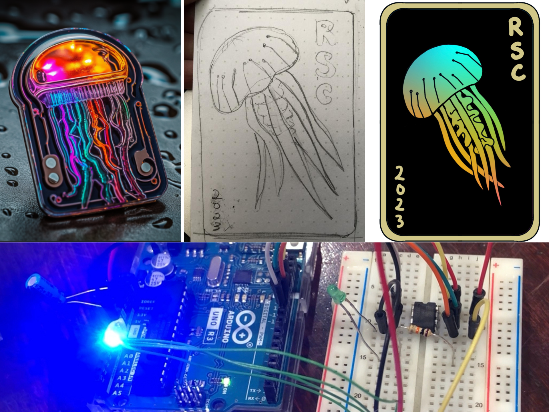
With the inspiration for badge life and the PCB prototyping process already explained, we’re ready to finally turn the design into something that’s manufacturable.
KiCad and Circuit Design
With everything figured out, it’s time to start using a circuit design tool. I’ll use KiCad because it’s great, and it’s free. I have used Eagle in the past, which is another great option hobbyists (free for limited features). I like KiCad more because it has a great open source community that has continued to contribute to and improve the tool.
There’s also Altium and Mentor Graphics, both expensive but more likely to be used at a “real” company.
A couple years ago, I gave a 4-hour PCB design workshop for laypeople (at The Diana Initiative). The original version of the workshop used Eagle, the more updated version used KiCad. Hit me up if you want me to give this workshop at your conference. :)
Within KiCad (or for that matter, any other PCB design tool), we have two main parts: schematic and PCB layout.
The schematic shows a symbolic representation of our circuit. The PCB layout shows the actual physical layout of our circuit. We’ll first make the schematic, and then ‘forward’ it to our PCB layout.
Circuit Recap
I know, I just spent an entire blog post talking about this, but let’s quickly recap what we need to include in our schematic and PCB layout:
- Addressable RGB LEDs, which each need a connection to power, ground, and a data line (data in and out). We’ll probably have ~10 of them grouped around a fairly compact art design. These are pretty power hungry for a battery-powered design, but our artwork goals were more important in this case.
- The LEDs will be driven by an ATTiny (8 pin TSSOP package).
- This ATTiny needs to be programmed, so we’ll add a programming header (for us, and for future users).
- We need a boost converter which in our case requires an external inductor and capacitor. This could be all one package (for more money).
- We need a battery holder and battery, plus a switch to disconnect power when not in use. We’ll also have a micro USB option for power.
- Black light: we need a black light (UV) LED, voltage divider (resistor) and a button.
- A few miscellaneous things: A resistor and capacitor for the LEDs, per the Neopixel instructions. We need some ESD protection because these badges are going to be on lanyards brushing up against people’s shirts. And a few other pull-up and pull-down resistors.
Getting the Art from iPad to KiCad
Having finally finished the jellyfish artwork process (with all of its many LED-constraints and artistic nitpicking), it’s time to translate the artwork into a PCB footprint.
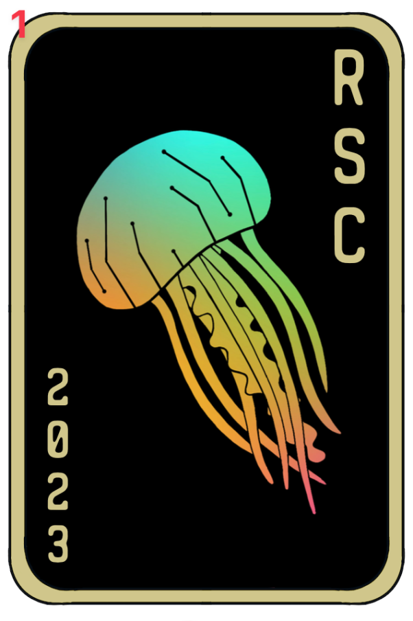
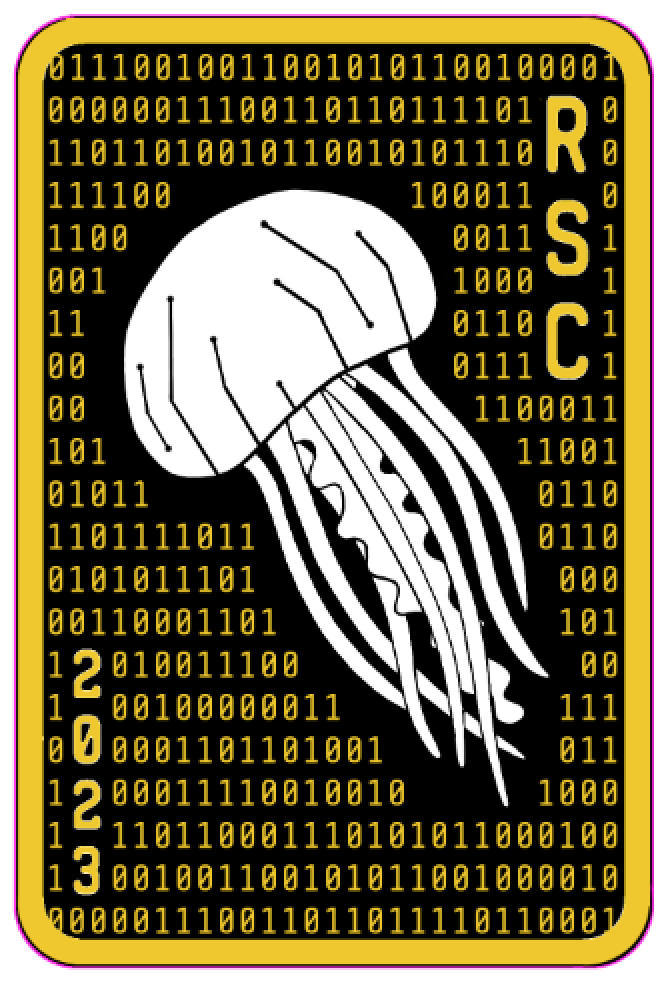
The artwork needs to be separated out into layers that correspond to the different layers of our eventual PCB:
- Silkscreen: the very top layer, in our case, this is white text.
- Solder mask: most boards are green (due to their green solder mask). Ours will be black. From an art perspective, this will be the outline of the jellyfish and the backdrop through which the rainbow LEDs shine through.
- Exposed copper layer: we will have exposed copper around the outside of the board, like the border of a playing card.
- Copper layer under solder mask: we’ll also have copper in a 1s and 0s pattern to add texture around the jellyfish.
And of course, copper is going to have a practical use in our design too, on the bottom layer (circuit traces between components, and footprints).
I did not separate these layers out on my iPad, but instead used GIMP to create a multi-layer design. I could have done some of this layer planning on my iPad, but I don’t have enough artistic talent to develop the design and separate the layers out at the same time. 😛
SVG2Shenzen
Okay, so I exported the design, separated out the layers on my laptop, now what?
Enter SVG2Shenzhen, which is an Inkscape extension for generating PCB art. The output is a footprint that you can include in your KiCad (or other) design. Footprints are discussed in more detail in the next section.
If you are unable to use it due to Inkscape version restrictions, check out SVG2Mod and Gingerbread.
After you install the plugin, you then have to “prepare the document” (set sizes, applicable PCB layers, etc.) Then you add the SVG versions of your artwork, and assign them to the right layers.
For the jellyfish art, the 1s and 0s and the outlines went on the F.Cu (front copper) layer, the solder mask jellyfish outline went on the F.Mask layer, and so on.
Take note of the layername definitions section, which points out something kind of unintuitive–depending on how you drew your design, you might have to specify your solder mask layers as being inverted.
Symbols and Footprints
We need a symbolic representation of the circuit (schematic) as well as a physical representation (layout).
For each component in our circuit, we need a schematic symbol for the schematic, and a board layout footprint (“land pattern”) for our PCB layout.
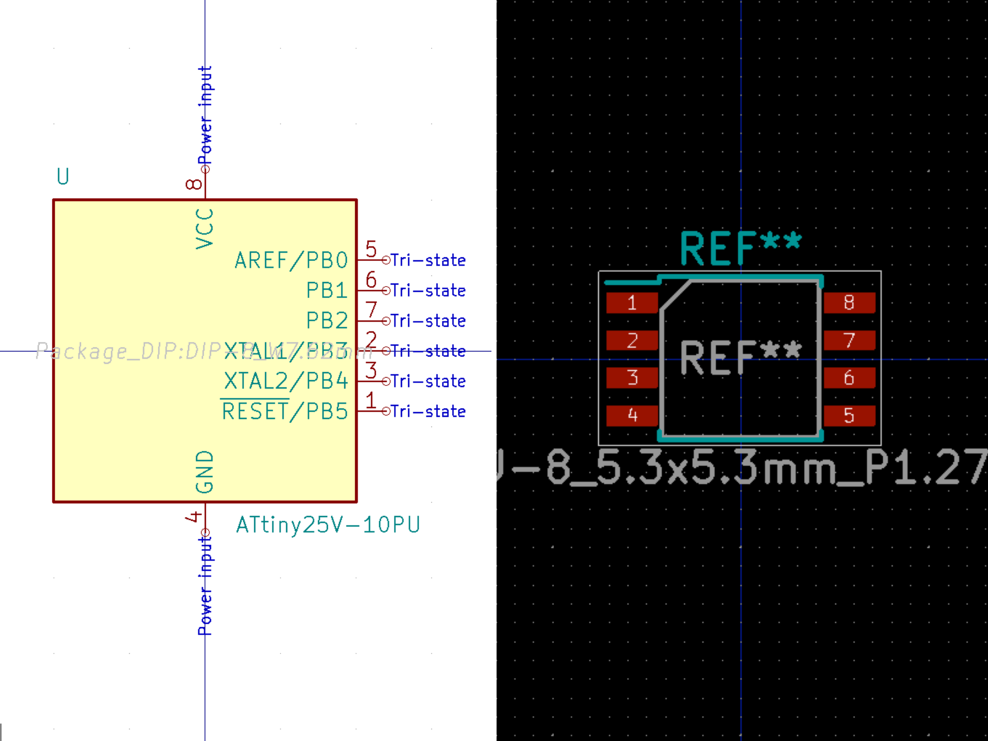
For standard components like resistors and capacitors, these will likely already exist within standard part libraries included in KiCad. This is also true of standard packages like SOD-123 and headers.
If we don’t have the symbol and footprint for a part, we have a couple different options:
- We can make them if they don’t exist, but this requires a LOT of double-checking. Especially for the footprint, as not only do you need to match the dimensions of all the pads exactly, but there are also multiple layers. Plus, it’s easy to accidentally mirror the design.
- You can also find components online, at sites like SnapEDA and Mouser’s Component Search. Again, just because it’s premade doesn’t mean you’re off the hook for review! Make sure that the symbol and especially the footprint match the datasheet exactly.
We will need to go through our entire component list (also known as a BOM or bill of materials) and make sure we have a symbol and footprint for each: LEDs, ATTiny, boost converter, inductor, capacitors, resistors, battery holder, black light LED, button, switch, etc.
Speaking of review: in a “normal” environment you’d have schematic and board design review meetings and processes. As a single person working on it, it’s easier to make mistakes that would otherwise be caught by these processes so be thorough and look for those who can help if possible.
By the end of this step, you should have a schematic that you have checked for both high-level design issues, and DRC (design rules check) for unconnected “nets” (wired connections).
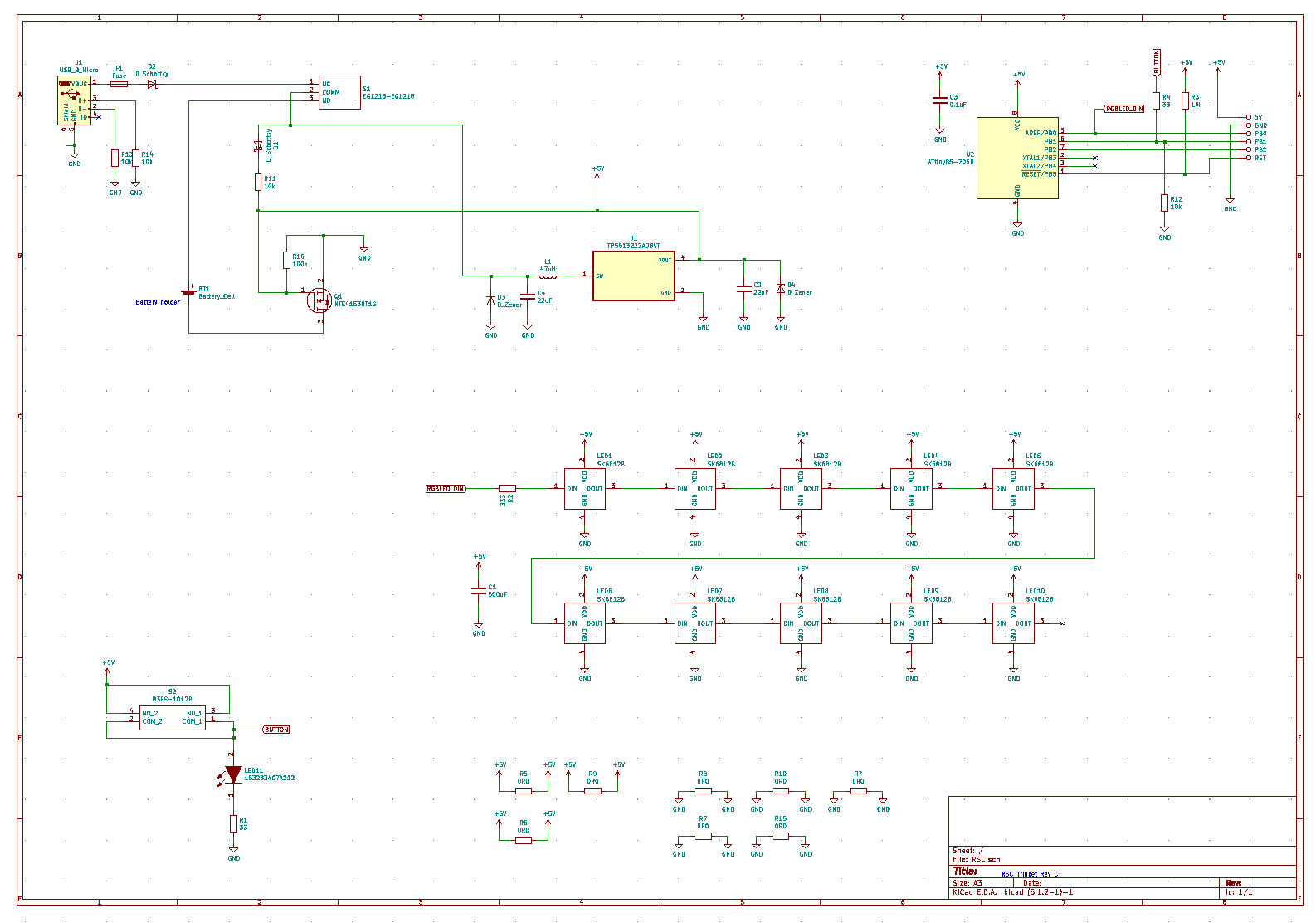
Then, you should forward this to the PCB layout view, and layout your board. It will start out looking like this. No board outline, no order, just vibes and nets. 😌
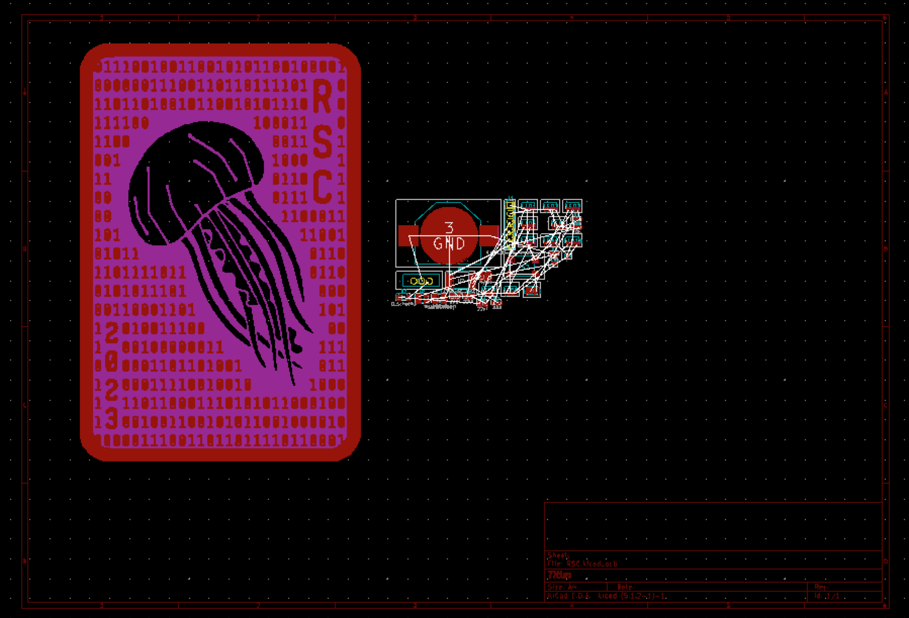
Each white line between footprint pins corresponds to a connection that you made in the schematic. And once you have done a lot of routing and re-routing and even MORE re-routing, the layout will look like this:
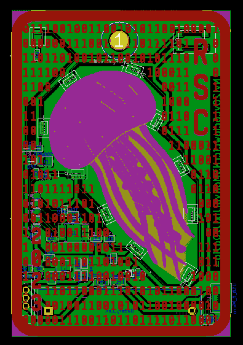
This blog post is already long enough, but suffice to say it took a lot of trial and error to get to this point.
One of the major constraints was, again, aesthetic: no traces on the top of the board, so that the top only showed the intended artwork (jellyfish and “1s and 0s”).
This required some creative designing for the LEDs, which had to be chained together:
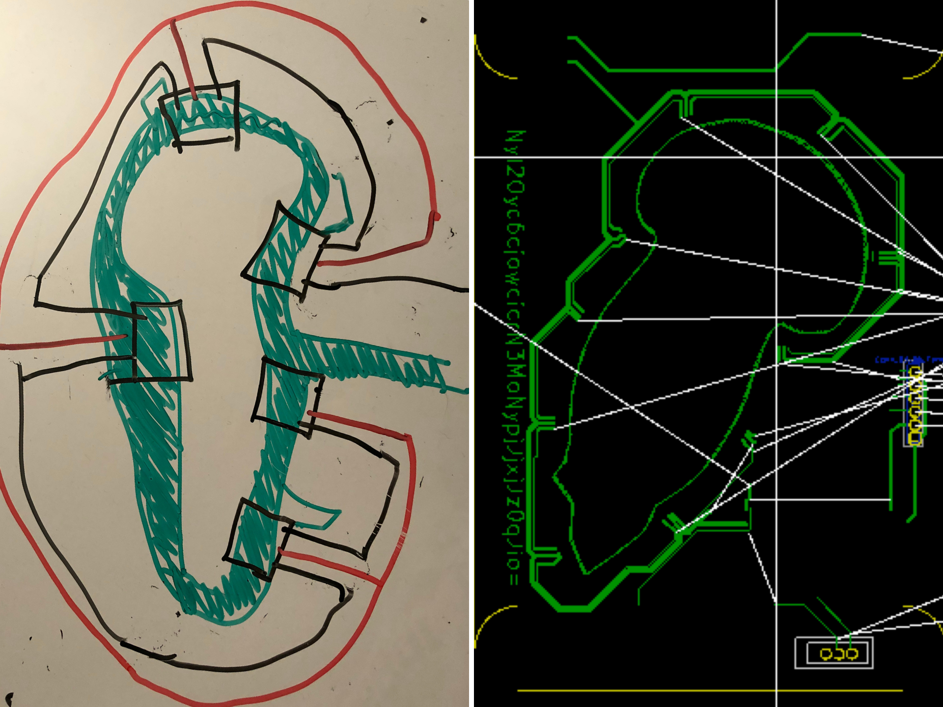
Once you’re done there, it’s time for another review and DRC check.
You’ll also want to make sure that your board design rules match what your intended board manufacturer’s equipment is capable of (ideally you have determined this before your board is entirely designed, but hey, it’s a blog post! I can add on footnotes whenever I’d like).
If you think I’m skipping over details here, you’d be correct. The specifics of how you connect, layout, and check the schematic and layout is what my 4-hour Diana Initiative workshop was about. So again, hit me up if you want me to present it at your event.
Ordering Your PCBs
Finally, time to get some PCBs in hand, how exciting!
Once you’ve got your KiCad board layout done, and you’ve checked mistakes.badge.life to make sure you haven’t forgotten anything, it’s time to generate Gerber files.
Why are they called Gerber files? Apparently the format was originally developed by Gerber Scientific (and its founder Joseph Gerber) in the 1980s. The more you know.
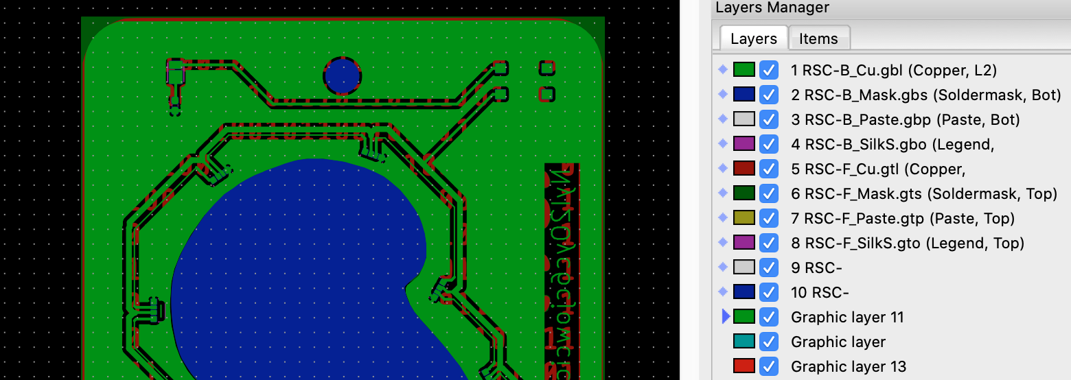
Gerber files are a set of files that specify the copper layers, the solder mask, drill information, etc. It’s what the manufacturing equipment needs to have in order to actually machine your boards. Think of it like CAD files for your PCBs (did anyone else have to write G-code in college?)
Depending on what PCB manufacturer (“board house”) you go with, they might expect certain file extensions. This can almost always be found on the board house’s website or on ordering page, so do a quick check beforehand.
How to Choose a Board House
There are a lot of options for PCB manufacturing. This could be a whole blog post in itself, but for the sake of keeping things (relatively) concise: as with many things, it’s a trade-off between time, cost, quality, and other limitations.
There are PCB manufacturers within the US (such as OSHPark and 4PCB) that will be slightly more expensive than their Chinese counterparts, but you generally spend less time and money in shipping.
There are many Chinese manufacturers like JLCPCB, PCBWay, and AllPCB. These are generally cheaper and faster production times, but you pay more with shipping, and of course it also takes longer to arrive.
Another thing to consider with timing is lead times. This is usually stated on the manufacturer’s website. Long lead times for domestic manufacturers meant that I chose JLCPCB for this project. JLCPCB also had the solder mask options I wanted, although this was true of most manufacturers because black solder mask is not uncommon. I would love to try OSHPark’s “after dark” styling sometime!
Some “real” engineering projects may not be able to offshore their PCB development for legal reasons (such as government contracts), and other projects might choose their manufacturer based on IP enforcement concerns.
Board Spins (and Why You Should Count on Having Several)
Each time you create a board design and have it manufactured, that’s a board spin.
You might think that the extensive prototyping phase with the actual components would be enough to not need multiple board revisions.
But you’d be wrong.
You’ll see later in this blog post that mistakes still existed in the design (due to a footprint error), and I had to do another board spin.
How does this affect you? Well, if all of your engineering projects always get done on time and under budget, you can skip ahead to the next section.
...
For everyone else: board spins should factor into both your schedule and your budget. Assume that you will need at least 2 or 3 board spins.
If your PCB manufacturer has a one week lead time, takes one week to ship to you, and you take one week to assemble and test the new design, then you need to factor in at least two 3+ week periods into your schedule. Of course, you’ll want to adjust that example to your own life. Maybe you have more or less discretionary testing time, etc.
Each board spin requires parts, so you’ll need to factor in DigiKey/Mouser/etc shipping times (and cost!) into your schedule and budget. And then of course, the cost of the boards themselves, plus shipping.
Save the fancy stuff for your last board spin
As mentioned, I chose JLCPCB due to long lead times at other manufacturers at the time of this project. They also had the design choices I wanted. Here’s a quick look at some of them:
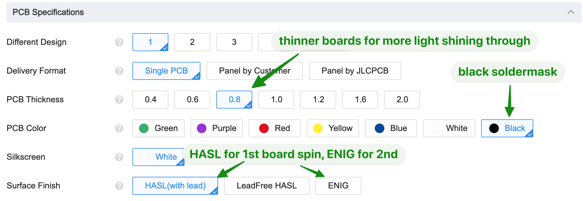
The eventual board design used “ENIG” finishing on the exposed copper layer, making it look more, well, copper-y.
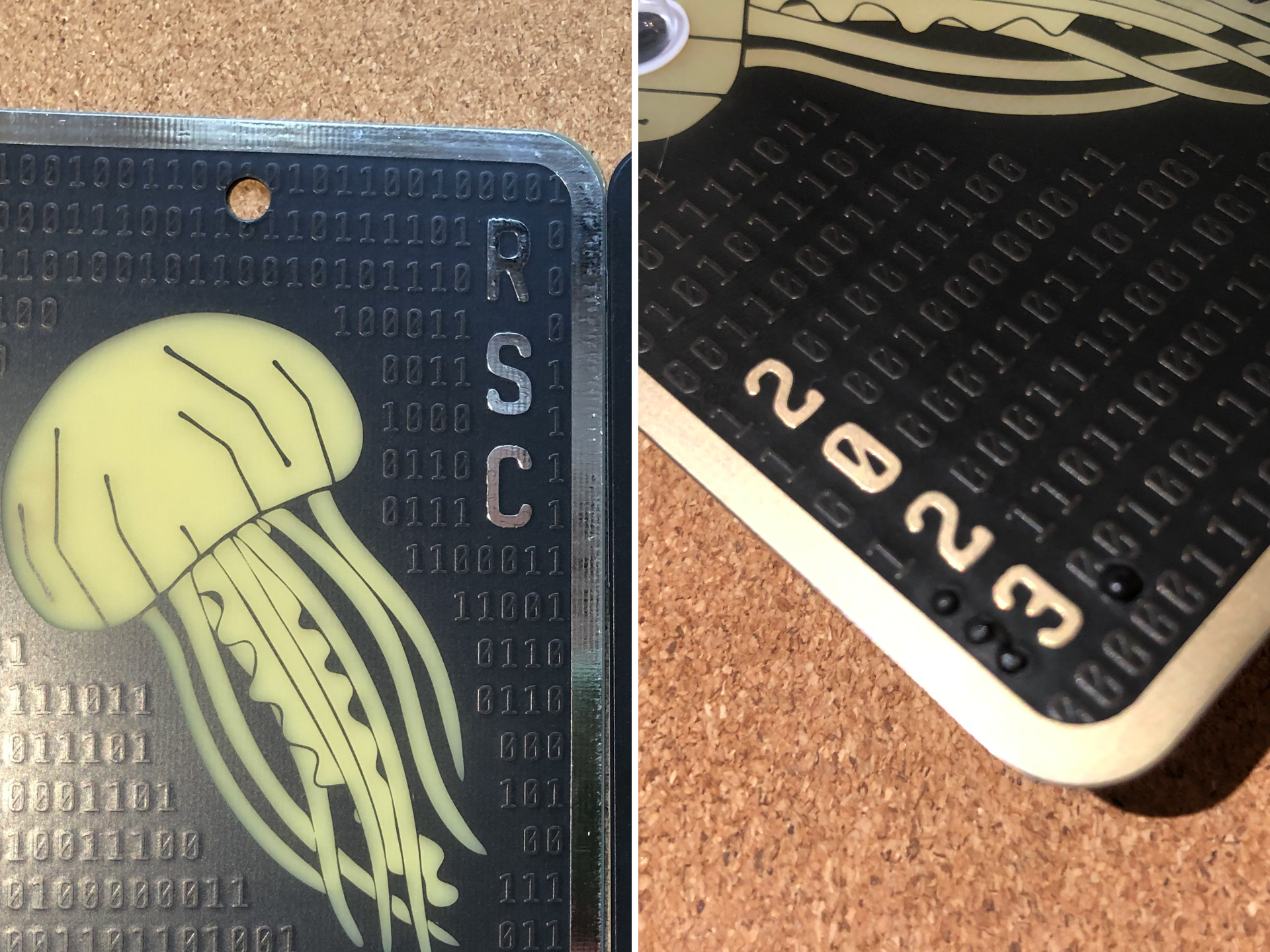
The default, cheaper option (HASL) looked more silver-y, which isn’t what I wanted from an art perspective. The cheapest option is also not lead-free, which is non-ideal for a badge with exposed metal (since people will be handling the badge a lot!)
But ENIG costs more, and adds to the turnaround time. Same goes for other variations from the norm: solder mask colors, and so on.
So: consider saving some of those finishing touches for your second or third board spin, to save a bit of time and money.
2023 Supply Chain: Not Great, Not Terrible
I am not a full-time hardware designer, so I really have no place complaining about my limited supply chain issues.
But I did run into some issues, and thought I’d mention a few pointers here.
First of all: Octopart to find parts.
I used to always buy from DigiKey (they are geographically close to me) but have since branched out to other options.
Second: join the BadgeLife Discord and ask for help. I joined this group after Defcon and learned about a bunch of alternative parts that would have saved me a lot of headache.
Board Bringup
“Board bringup” refers to the process of getting your PCBs, getting your components, assembling your board, and testing it.
That means powering it on for the first time–something I always reflexively cringe during–and hoping that you don’t let out the magic smoke.
That also means testing different functionality of the board, and (if you were working with others) passing a couple copies along to the software developers to start writing software.
In short: board bringup is where you’re going to find the mistakes that you missed earlier.
And yes, they will be expensive to fix.
Adapt and Overcome (Fixing Issues)
My first board spin was an order of 5 boards. During board bringup, the major issue I found was in one of the footprints.
About that “thoroughly check your footprints to make sure they’re right” advice I mentioned earlier: yeahhhh. Whoops.
As it turns out, someone else misread the datasheet for the LEDs the same way I did, resulting in a mirrored part. This required a second board spin.
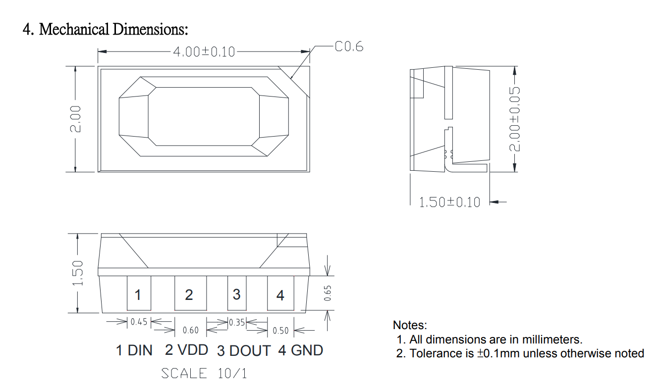
One other thing I did not expect, and that I did not run into until my second board spin, was FR4 watermarks.
I did not think of this beforehand, because this is my first design with exposed FR4. But! Most (all?) FR4 will have a watermark in the design indicating that it is the real deal, and not counterfeited.
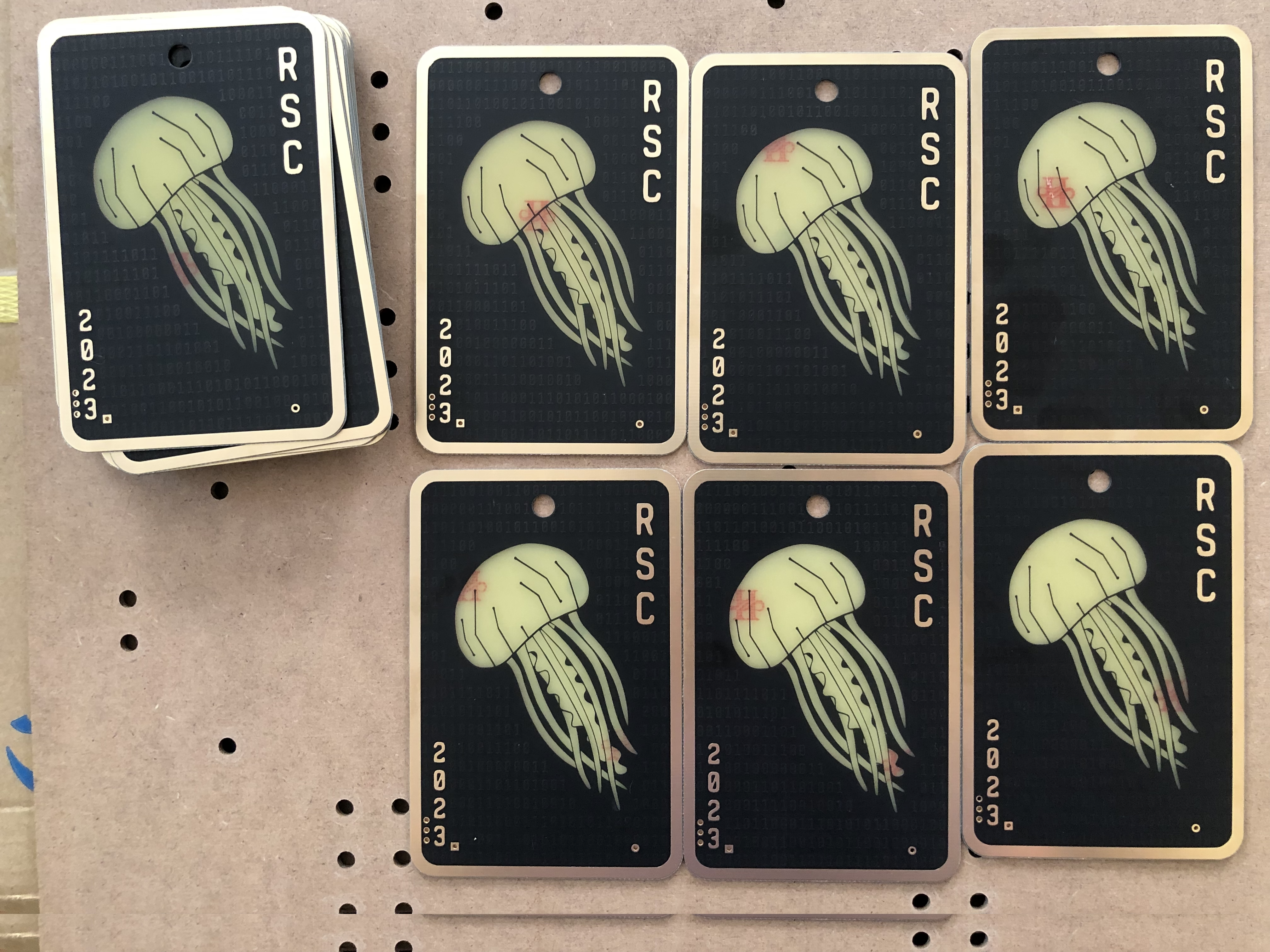
Nice for the board manufacturers, not nice for me. After some back and forth with customer service, they pointed out that this is discussed in their terms of sale. With about 50% of the FR4 exposed in my jellyfish design, I decided to buy a 2x overage of boards (i.e. 100 blank PCBs to create 50 final badges).
DIY Board Assembly
For boring supply chain and timing reasons I will not get into here: it did not work out schedule-wise to have the PCB manufacturer assemble my boards. Plus, there were a few steps (epoxy, etc) required after PCB assembly that I had to do at home anyway.
And, with typical engineering optimism, I decided to just do it myself.
(To those wondering about an alternative: you can often find manufacturing facilities in your city/state that will do assembly, or find a company/friend/makerspace that has a pick-and-place machine).
While this approach absolutely does not scale past 50 boards, it was a great learning opportunity.
It gave me flashbacks to my senior project, when we could not afford PCB assembly, so I hand-soldered three very intricate boards myself.
This time around, I had a reflow oven to help me. After ordering a stencil from the PCB manufacturer, I set up a workstation where a fresh PCB would be taped in place. The stencil would be placed (and secured) on top. Then, I’d spread a layer of solder paste and scrape it across the design with a flat edge.
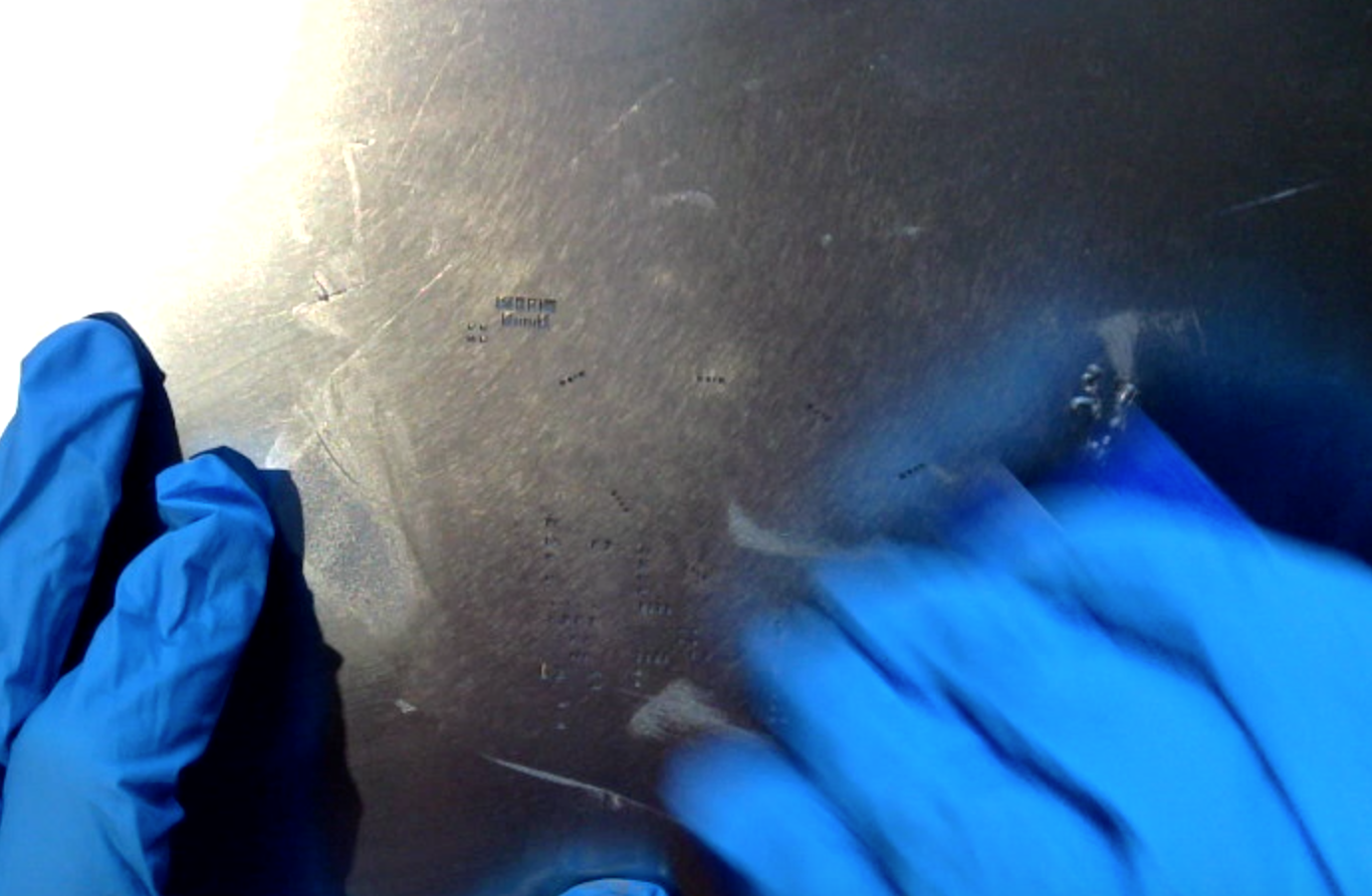
I watched several videos on Youtube in order to improve my technique: it’s a matter of getting the perfect Goldilocks amount of paste on each pad. I did not save the videos to link here, unfortunately, but I am grateful for them.
After hand placing the components with ESD-safe tweezers, I placed them in the T-962 reflow oven and ran the program. My partner and I replaced the original firmware of the reflow oven with one from Unified Engineering (per this Hackaday post), which is supposed to have better heating profiles. We also used an ultrasonic cleaner to clean the boards.
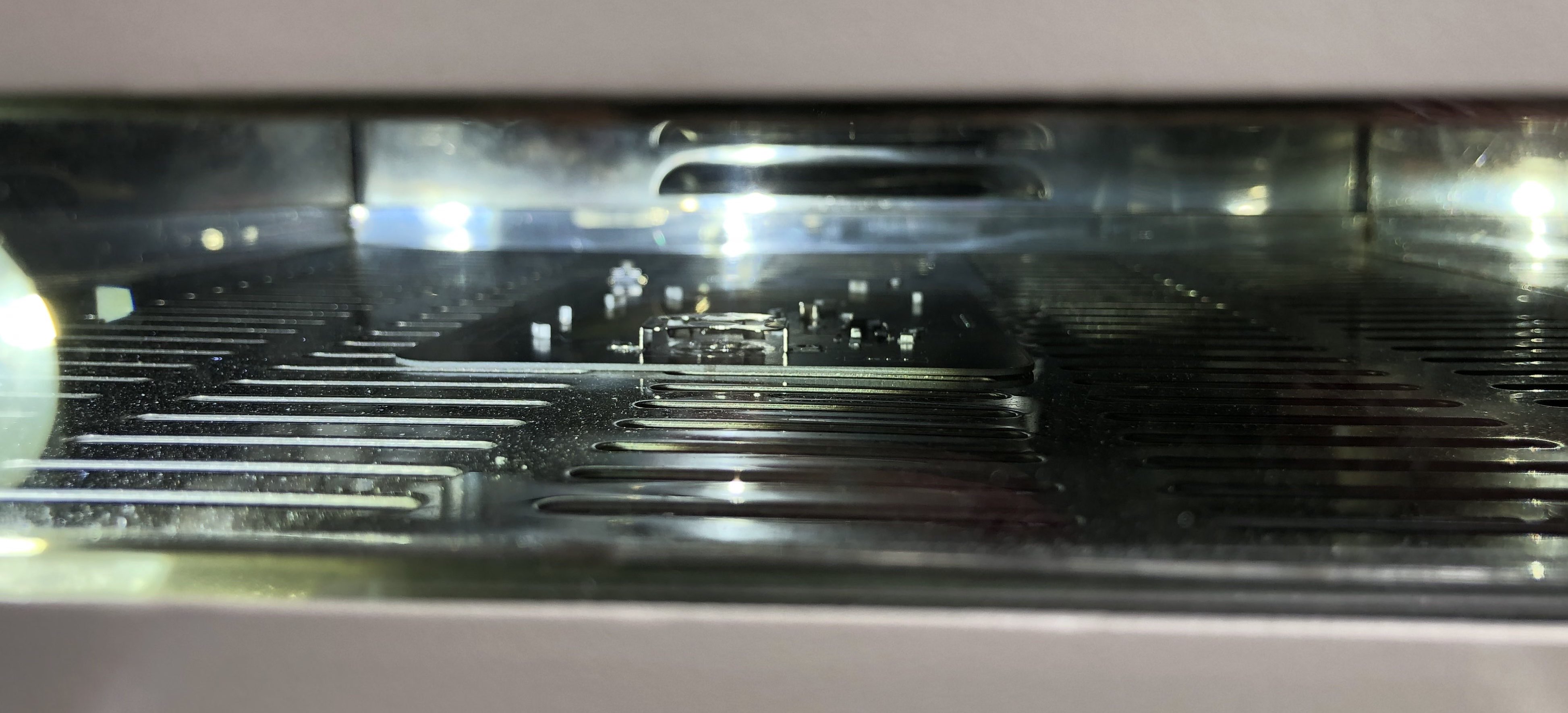
With all 50 boards done, I then added epoxy to the back. This is to help with the lighting effect. I used what I had on hand, which conveniently enough, included black hot glue and automotive-grade clear epoxy.
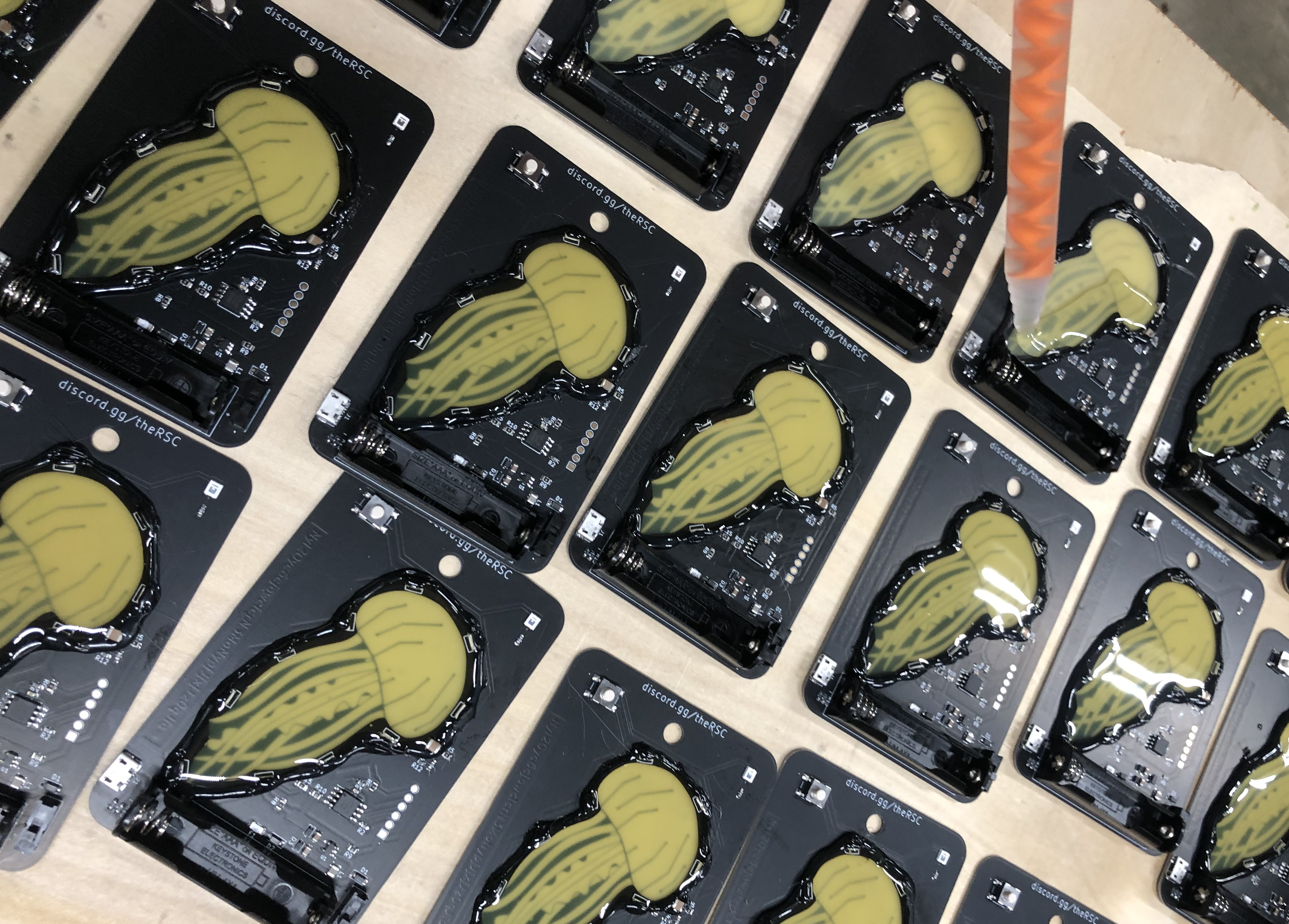
This was a high-stress part of the process: the epoxy has to be mixed properly to avoid uneven curing, and to avoid bubbles. And you have to move quickly enough from board to board to use all the epoxy before it cures. Phew!
If you are doing a smaller exposed area, you can just use clear hot glue and “reflow” it with a hair dryer or heat gun. But this is quite a large area to cover with hot glue, which is why I used epoxy instead.
I also used black nail polish to cover up the through hole components on the front side of the board. You know, for ✨aesthetic✨.
Final Outcome, DEFCON 31, and Takeaways
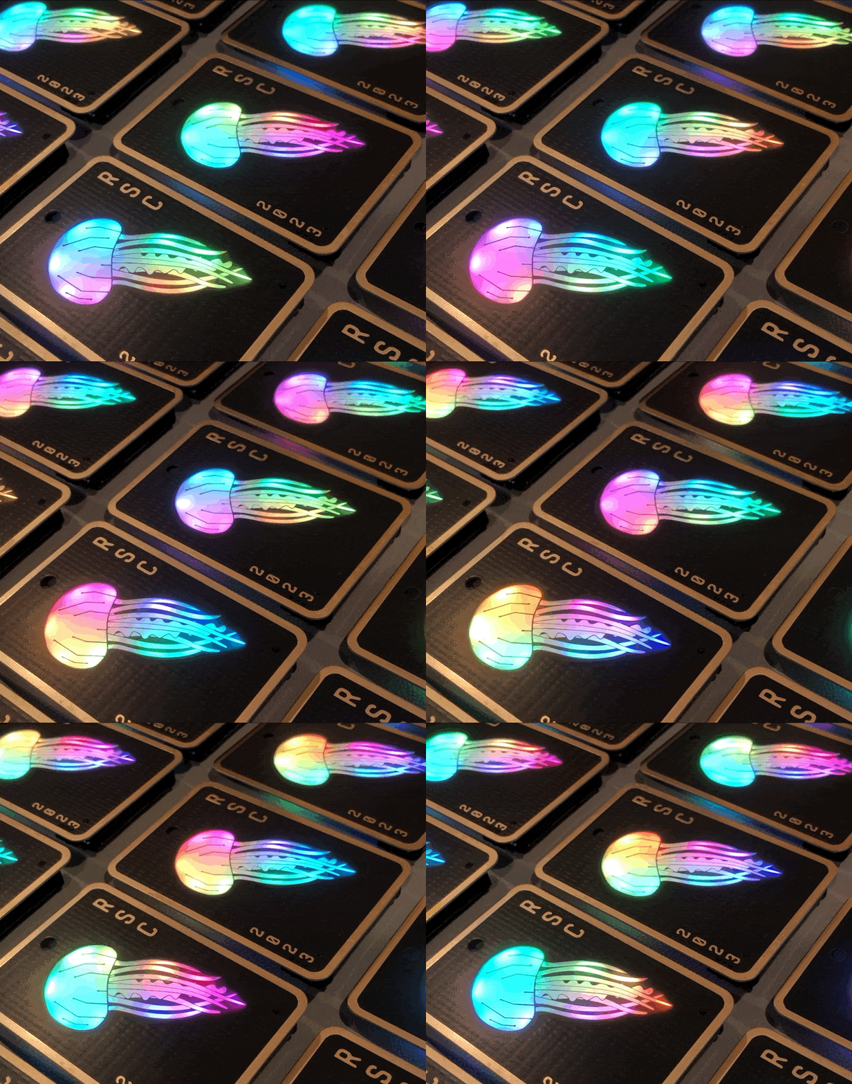
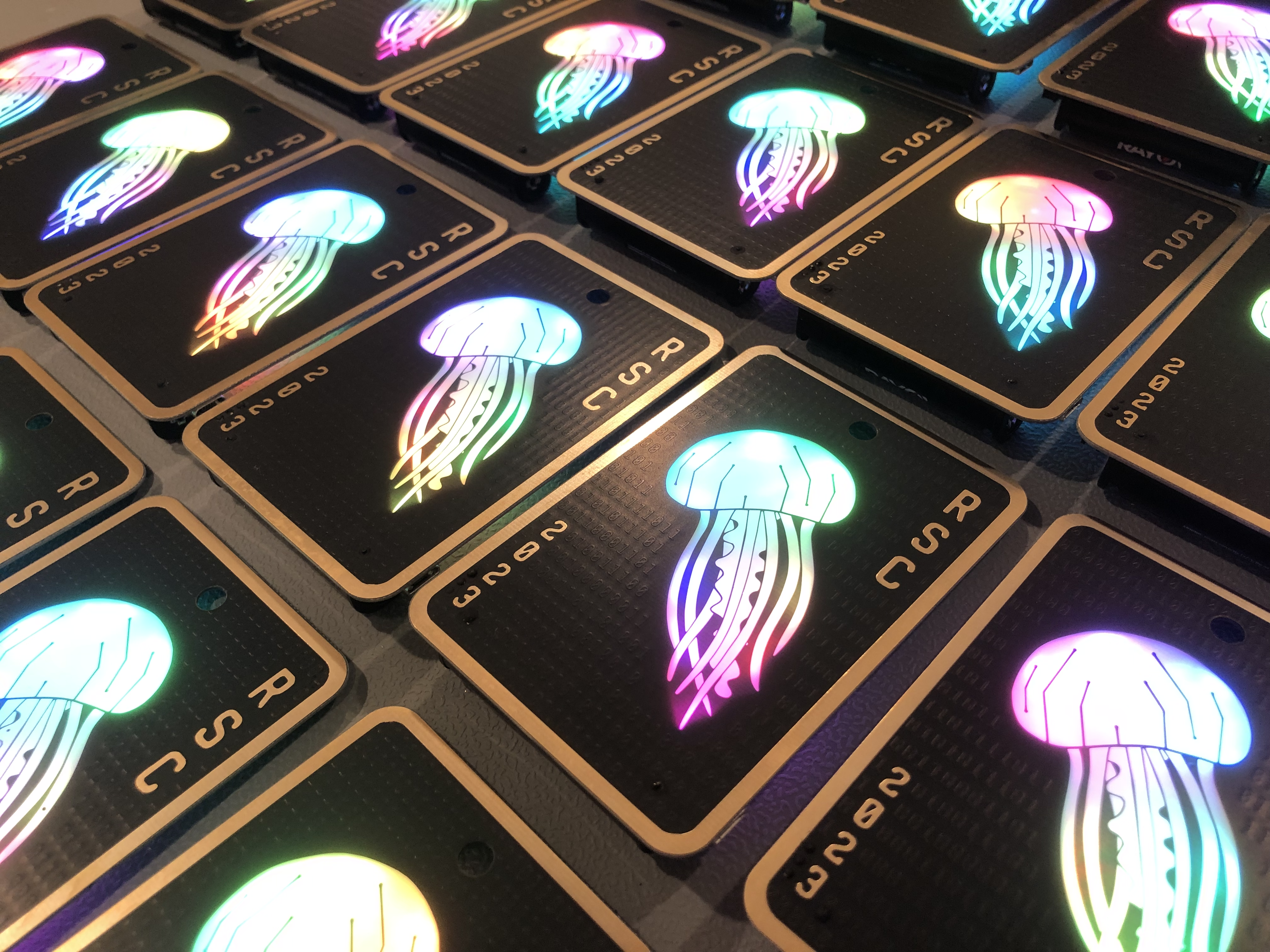
Here’s the part where I do a victory lap with lots of photos! I’m so happy with how the art came out.
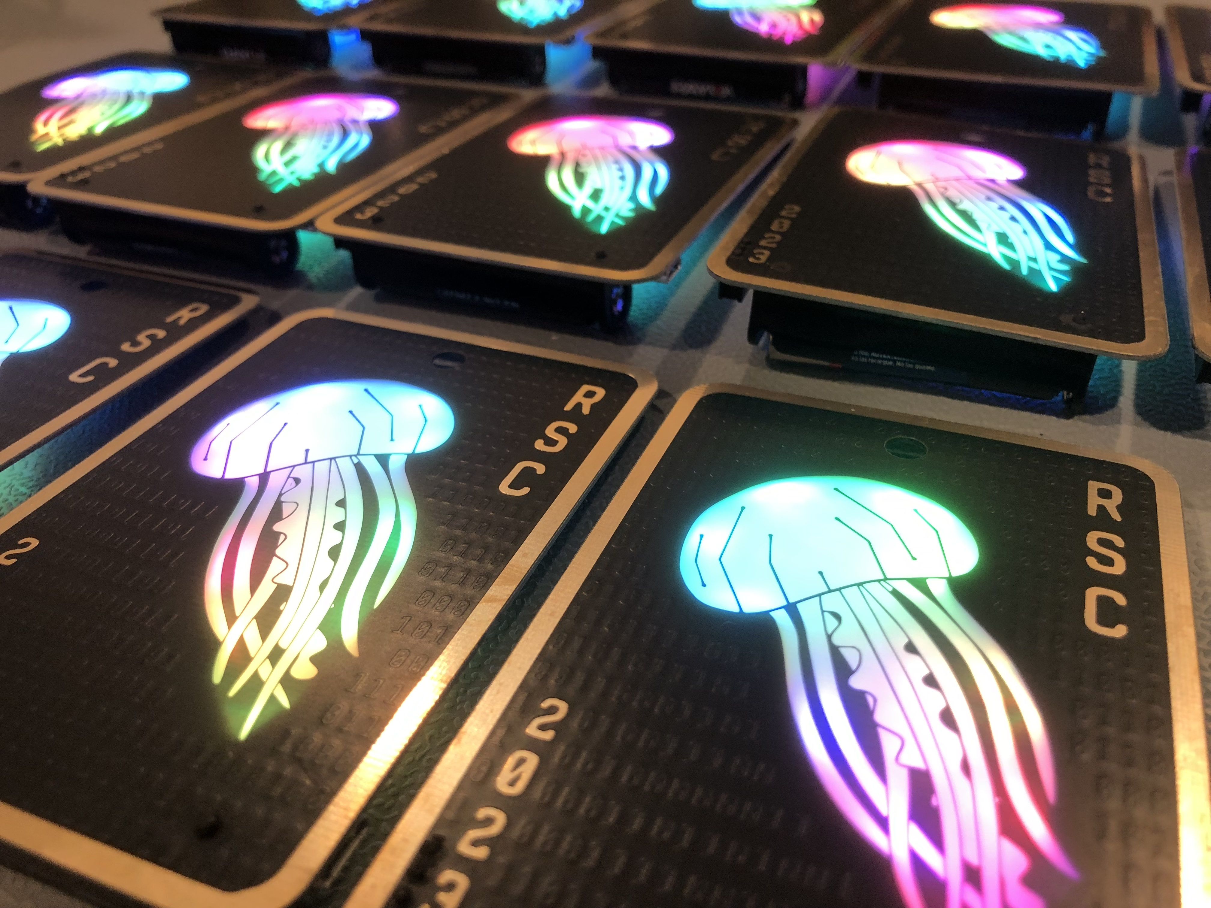

I ended up doing a third revision with a better power circuitry design (less heat through one component, but still maintaining reverse-polarity protection).
If I did this again, I would start sooner 😛 and maybe use less power-hungry LED designs. But overall, I’m very happy with how it turned out, and am really glad that I experimented with the backlit LEDs. I’ve been wanting to try it out for a very long time, and this was a great project to test with.
If you made it this far, thank you for reading! I hope you have found this series useful or interesting, and encourage you to try out your own circuit designs.
